|
|
|
|
 |
|
tenx MCU
> 8051 Series
> High Efficiency
|
|
| |
| TM52F5284/5288 |
|
|
8051 Core Architecture Microcontroller with Touch Key Function
|
|
TM52F5284/5288 Datasheet (*.pdf)
|
|
Description:
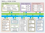
TM52 Series F5284 and F5288 are versions of a new, fast 8051 architecture for an 8-bit microcontroller single chip with an instruction set fully compatible with industry standard 8051, and retains most 8051 peripheral function block. Typically, the TM52-F5284/88 executes instructions six times faster than the traditional 8051 architecture.
|
|
Feature:
FEATURES
1. Standard 8051 Instruction set, fast machine cycle
. Executes instructions six times faster than the traditional 8051
2. 16K Bytes Flash Program Memory
. Support “ In Circuit Programming ” (ICP) or “ In System Programming ”
(ISP) for the Flash code
. Byte Write “ In Application Programming ” (IAP) mode is convenient
as Data EEPROM access
. Code Protection Capability
3. Total 512 Bytes SRAM (IRAM + XRAM)
. 256 Bytes IRAM in the 8051 internal data memory area
. 256 Bytes XRAM in the 8051 external data memory area
(accessed by MOVX Instruction)
4. Four System Clock type Selections
. Fast clock from 1~6 MHz Crystal
. Fast clock from Internal RC (7.3728 MHz)
. Slow clock from 32768 Hz Crystal
. Slow clock from Internal RC (80 KHz)
. System clock can be divided by 1/2/4/16 option
5. 8051 Standard Timer – Timer0/1/2
. 16-bit Timer0, also supports T0O clock output for Buzzer application
. 16-bit Timer1
. 16-bit Timer2, also supports T2O clock output for Buzzer application
6. 15-bit Time3
. Clock source is Slow clock
. Interrupt period can be clock divided by 32768/16384/8192/128 option
7. 8051 Standard UART
. One Wire UART option can be used for ISP or other application
8. Two independent "8+2" bits PWMs with prescaler/period-adjustment
9. SPI Interface
. Master or Slave mode selectable
. Programmable transmit bit rate
. Serial clock phase and polarity options
. MSB-first or LSB-first selectable
10. 12-Channel Touch Key (F5284 only)
11. 12-bit ADC with 10 Channels External Pin Input and 2 Channels Internal Reference Voltage
12. LCD Controller/Driver
. 1/2~1/8 Duty
. Max. 8 COM x 20 SEG
. 1/3 or 1/4 LCD Bias
. 8 Brightness Level selection
13. LED Controller/Driver
. 1/2~1/8 Duty
. Max. 8 COM x 20 SEG
. 40mA High Sink COM
. Active High or Active Low Common Output
. COM Dead Time option
14. 11 Sources, 4-level Priority Interrupt
. Timer0/Timer1/Timer2/Timer3 Interrupt
. INT0/INT1 Falling-Edge/Low-Level Interrupt
. Port1 Pin Change Interrupt
. UART TX/RX Interrupt
. P4.7 (INT2) Interrupt
. ADC/Touch Key Interrupt
. SPI Interrupt
15. Pin Interrupt can Wake up CPU from Power-Down (Stop) mode
. P3.2/P3.3 (INT0/INT1) Interrupt & Wake-up
. P4.7 (INT2) Interrupt & Wake-up
. Each Port1 pin can be defined as Interrupt & Wake-up pin (by pin change)
16. Max. 42 Programmable I/O pins
. CMOS Output
. Pseudo-Open-Drain, or Open-Drain Output
. Schmitt Trigger Input
. Pin Pull-up can be Enable or Disable
17. Independent RC Oscillating Watchdog Timer
. 400ms/200ms/100ms/50ms Selectable WDT Timeout options
18. Five types Reset
. Power on Reset
. Selectable External Pin Reset
. Software Command Reset
. Selectable Watchdog Timer Reset
. Selectable Low Voltage Reset
19. 3-level Low Voltage Reset
. 1.9V/2.3V/2.9V (can be disabled)
20. 1-level Low Voltage Detect
. 2.3V (can be disabled)
21. Four Power Saving Operation Modes
. Fast/Slow/Idle/Stop Mode
22. On-chip Debug/ICE interface
. Use P1.2/P1.3 pin
. Share with ICP programming pin
23. Operating Voltage and Current
. VCC = 2.9V ~ 5.5V @FSYSCLK = 7.3728 MHz
. VCC = 1.9V ~ 5.5V @FSYSCLK = 4 MHz
. ICC = 3.5uA @Stop mode, LVR enable, MODE3V = 0, PWRSAV = 1, VCC = 5V
. ICC = 1.2uA @Stop mode, LVR enable, MODE3V = 0, PWRSAV = 1, VCC = 3V
. ICC = 1.2uA @Stop mode, LVR enable, MODE3V = 1, PWRSAV = 1, VCC = 3V
24. Operating Temperature Range
–40*C ~ +85*C
25. Package Types
. DIP 32-pin (600 mil)
. SOP 32-pin (300 mil)
. QFP 44-pin (10x10 mm)
|
|
|
|
|
|
|