|
|
|
|
 |
|
tenx MCU
> 8051 Series
> Low Power
|
|
| |
| TM52F2260 |
|
|
8051 Core Architecture Microcontroller
|
|
TM52F2260 Datasheet (*.pdf)
|
|
Description:
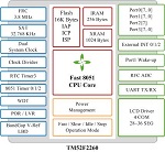
TM52 series F2260 is a version of a new, fast 8051 architecture for an 8-bit microcontroller single chip with an instruction set fully compatible with industry standard 8051, C language development platform, and retains most 8051 peripheral functional block. Typically, the TM52-F2260 executes nstructions six times faster than the traditional 8051 architecture.
|
|
Feature:
FEATURES
1. Standard 8051 Instruction set, fast machine cycle
. Executes instructions six times faster than the traditional 8051.
2. 16K Bytes Flash Program Memory
. Support " In Circuit Programming " (ICP) or " In System Programming " (ISP) for the Flash code
. Byte Write " In Application Programming " (IAP) mode is convenient as Data EEPROM access
. Code Protection Capability
3. Total 1280 Bytes SRAM (IRAM + XRAM)
. 256 Bytes IRAM in the 8051 internal data memory area
. 1024 Bytes XRAM in the 8051 external data memory area (accessed by MOVX Instruction)
4. Three System Clock type Selections
. Fast clock from Internal RC (FRC, 3.75MHz @VDD=3V)
. Slow clock from 32768Hz Crystal (SXT)
. Slow clock from RFC
. System Clock can be divided by 1/4/16/64 option
. System Clock output pin (TCO) for EL / IR application
5. 8051 Standard Timer – Timer0 / 1 / 2
. 16-bit Timer0, also supports RFC clock input counting
. 16-bit Timer1, also supports T1O / T1B clock output for Buzzer / IR application
. 16-bit Timer2, also supports T2O clock output for Buzzer / IR application
6. 23-bit Timer3 used for Real Time 32768Hz Crystal counting
. ± 0.5 ppm ~ 61 ppm interrupt rate adjustable
. MSB 8-bit overflow auto-reload
. 0.25 sec, 0.5 sec, 1.0 sec or overflow Interrupt
7. 9-Sources, 4-level priority Interrupt
. Timer0 / Timer1 / Timer2 / Timer3 Interrupt
. INT0 / INT1 Falling-Edge / Low-Level Interrupt
. Port1 Pin Change Interrupt
. UART TX/RX Interrupt
. P2.7 (INT2) Interrupt
8. Pin Interrupt can Wake up CPU from Power-Down (Stop) mode
. P3.2 / P3.3 (INT0 / INT1) Interrupt & Wake-up
. P2.7 (INT2) Interrupt & Wake-up
. Each Port1 pin can be defined as Interrupt & Wake-up pin (by pin change)
9. 8051 Standard UART
. One Wire UART option can be used for ISP or other application
10. Max. 25 Programmable I/O pins
. CMOS Output
. Pseudo-Open-Drain, or Open-Drain Output
. Schmitt Trigger Input
. Pin Pull-up can be Enabled or Disabled
11. Resistance to Frequency Converter (RFC)
. RFC clock divided by 1/4/16/64 signal can be assigned as Timer0 event count input
. RFC clock can be used as System clock source
12. LCD Controller / Driver
. 1/3 or 1/4 Duty
. 4 COM, 28 ~ 36 SEG
. 1/3 Bias, VL1 = VBAT / 3
. Frame Rate = 40Hz ~ 90Hz
13. BandGap Voltage Reference for Low Battery Detection (LBD)
. Detect VBAT voltage level from 2.5V to 3.1V
14. Built-in tiny current LDO Regulator for chip internal power supply (VDD)
. VDD voltage level can be set from 1.2V to 1.9V
15. Watch Dog Timer based on System Clock
. Running in Fast / Slow Mode, Stop counting in Idle / Stop Mode
. 32K or 64K counts overflow Reset
16. 5-types Reset
. Power on Reset
. Selectable External Pin Reset
. Selectable Watch Dog Reset
. Software Command Reset
. Selectable Battery Low Voltage Reset (when VBAT < 1.6V)
17. 4-types Power Operation Modes
. Fast / Slow / Idle / Stop Mode
18. On-chip Debug / ICE interface
. Use P1.2 / P1.3 pin
. Share with ICP programming pin
19. Operating Voltage and Current
. VBAT = 2.0V ~ 4.2V
. 0.3uA LCD Current @VBAT = 3V
. 0.1uA LVR Current @VBAT = 3V
. 0.6uA 32K Crystal and System Clock Current @VDD = 1.5V
. Total 1.0uA Idle mode Current with LCD on and LVR on, @VBAT = 3V,
VDD = 1.5V
20. Operating Temperature Range
. –40°C ~ +85°C
21. 64-pin LQFP Package
|
|
|
|
|
|
|